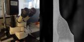
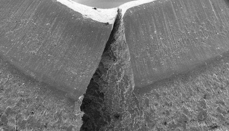
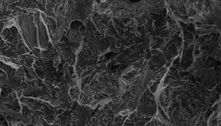
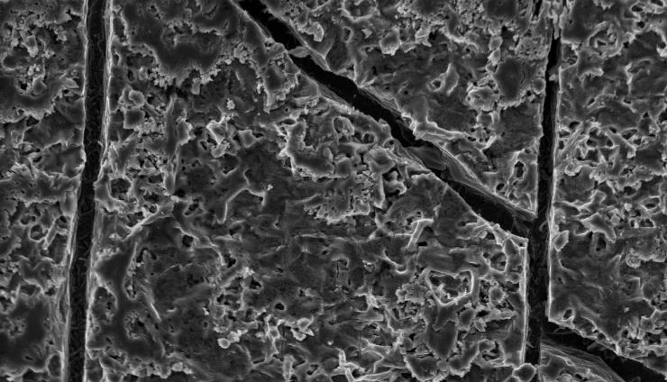
The SEM (Scanning Electron Microscope) is a very useful tool in micro and nano-structural investigation. It allows the study of high magnification of surfaces (fractures, topography).
It can reach 30000x compared to the 1000x of conventional optical microscopy while keeping the depth of field and the three-dimensionality of the image.The coupling of the EDX microprobe to the SEM also makes it possible to identify the chemistry of very small components such as inclusions and surface coatings.
Users
R&D Centres Technicians
Quality Managers
Production Managers
Instruments
SEM LEO 438 VP
Resolution: High pressure mode 4.0 nm
Low pressure mode 6.0 nm
Acceleration voltage: from 300 V to 30 kV
Filament current: from 1pA to 500nA
Magnifications: from 15x to 300kx
Filament: Tungsten (W)
Room size:190x300x265 mm HxLxP
Movement of the motorized stage on 5 axes
EDX BRUKER QUANTAX COMPACT MICROPROBE with X-Flash 610 Minidetector
Xflash 610 Mini Detector with 10mm2 active area
Resolution ≤ 126eV@MnKα
Peltier Cell cooling
Software Esprit Compact